Electrical assemblies useful in PV and power electronics
Extends from PVSystems.Icons.AssembliesPackage (Icon for packages of assemblies).
| Name | Description |
|---|---|
| Basic ideal H-bridge topology (averaged) | |
| Basic ideal H-bridge topology (switched) | |
| Bidirectional Buck Boost converter | |
| Bidirectional Buck Boost for battery USB interface |
 PVSystems.Electrical.Assemblies.HBridge
Basic ideal H-bridge topology (averaged)
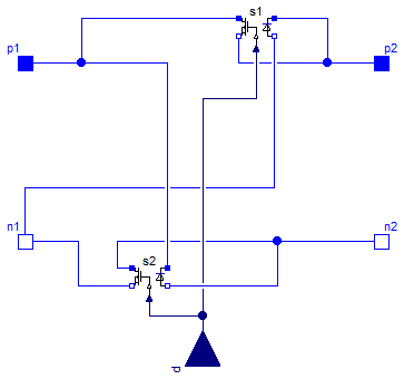
This model further composes IdealAverageCCMSwitch to form a typical H-bridge configuration from which a 1-phase inverter can be constructed. This model is based in averaged switch models.
Extends from Interfaces.TwoPort (Common interface for power converters with two ports), PVSystems.Icons.ConverterIcon (Icon for power converter models).
| Type | Name | Default | Description |
|---|---|---|---|
| replaceable model SwitchModel | CCM1 | ||
| Type | Name | Description |
|---|---|---|
| PositivePin | p1 | Positive pin of the left port (potential p1.v > n1.v for positive voltage drop v1) |
| NegativePin | n1 | Negative pin of the left port |
| PositivePin | p2 | Positive pin of the right port (potential p2.v > n2.v for positive voltage drop v2) |
| NegativePin | n2 | Negative pin of the right port |
| input RealInput | d | |
| replaceable model SwitchModel | ||
 PVSystems.Electrical.Assemblies.HBridgeSwitched
Basic ideal H-bridge topology (switched)
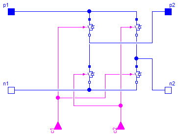
This model further composes IdealTwoLevelBranch to form a typical H-bridge configuration from which a 1-phase inverter can be constructed. This model is based on discrete switch models.
Extends from Interfaces.TwoPort (Common interface for power converters with two ports), PVSystems.Icons.ConverterIcon (Icon for power converter models).
| Type | Name | Description |
|---|---|---|
| PositivePin | p1 | Positive pin of the left port (potential p1.v > n1.v for positive voltage drop v1) |
| NegativePin | n1 | Negative pin of the left port |
| PositivePin | p2 | Positive pin of the right port (potential p2.v > n2.v for positive voltage drop v2) |
| NegativePin | n2 | Negative pin of the right port |
| input BooleanInput | c1 | |
| input BooleanInput | c2 |
 PVSystems.Electrical.Assemblies.BidirectionalBuckBoost
Bidirectional Buck Boost converter
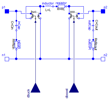
Bidirectional buck boost converter
Extends from Interfaces.TwoPort (Common interface for power converters with two ports), PVSystems.Icons.ConverterIcon (Icon for power converter models).
| Type | Name | Default | Description |
|---|---|---|---|
| replaceable model SwitchModel | CCM1 | ||
| Power stage | |||
| Capacitance | Cin | Input capacitance [F] | |
| Resistance | Rcin | Series resistance of input capacitor [Ohm] | |
| Capacitance | Cout | Output capacitance [F] | |
| Resistance | Rcout | Series resistance of output capacitor [Ohm] | |
| Inductance | L | Inductance [H] | |
| Resistance | RL | Series resistance of inductor [Ohm] | |
| Initialization | |||
| Voltage | vCin_ini | 0 | Guess for initial voltage of Cin [V] |
| Voltage | vCout_ini | 0 | Guess for initial voltage of Cout [V] |
| Current | iL_ini | 0 | Guess for initial current of L [A] |
| Switches | |||
| Real | dmax | 1 | Maximum duty cycle [1] |
| Real | dmin | 1e-3 | Minimum duty cycle [1] |
| Type | Name | Description |
|---|---|---|
| PositivePin | p1 | Positive pin of the left port (potential p1.v > n1.v for positive voltage drop v1) |
| NegativePin | n1 | Negative pin of the left port |
| PositivePin | p2 | Positive pin of the right port (potential p2.v > n2.v for positive voltage drop v2) |
| NegativePin | n2 | Negative pin of the right port |
| replaceable model SwitchModel | ||
| input RealInput | dbuck | Buck control voltage |
| input RealInput | dboost | Boost control voltage |
 PVSystems.Electrical.Assemblies.CPMBidirectionalBuckBoost
Bidirectional Buck Boost for battery USB interface
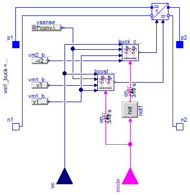
Bidirectional buck boost converter
Extends from Interfaces.TwoPort (Common interface for power converters with two ports), PVSystems.Icons.ConverterIcon (Icon for power converter models).
| Type | Name | Default | Description |
|---|---|---|---|
| Power stage | |||
| Capacitance | Cin | Input capacitance [F] | |
| Capacitance | Cout | Output capacitance [F] | |
| Inductance | L | Inductance [H] | |
| Resistance | RL | Series resistance of inductor [Ohm] | |
| Initialization | |||
| Voltage | vCin_ini | 0 | Guess for initial voltage of Cin [V] |
| Voltage | vCout_ini | 0 | Guess for initial voltage of Cout [V] |
| Current | iL_ini | 0 | Guess for initial current of L [A] |
| CPM modulator | |||
| Resistance | Rf | Equivalent sensing resistance [Ohm] | |
| Frequency | fs | Switching frequency [Hz] | |
| Voltage | Va_buck | Articial ramp amplitude for buck CPM [V] | |
| Voltage | Va_boost | Articial ramp amplitude for boost CPM [V] | |
| Type | Name | Description |
|---|---|---|
| PositivePin | p1 | Positive pin of the left port (potential p1.v > n1.v for positive voltage drop v1) |
| NegativePin | n1 | Negative pin of the left port |
| PositivePin | p2 | Positive pin of the right port (potential p2.v > n2.v for positive voltage drop v2) |
| NegativePin | n2 | Negative pin of the right port |
| input RealInput | vc | Buck control voltage |
| input BooleanInput | mode | Boost control voltage |
 PVSystems.Electrical.Assemblies.HBridge.SwitchModel

| Type | Name | Default | Description |
|---|---|---|---|
| Real | dmin | 1e-3 | Minimum duty cycle [1] |
| Real | dmax | 1 | Maximum duty cycle [1] |
| Type | Name | Description |
|---|---|---|
| PositivePin | p1 | Positive pin of the left port (potential p1.v > n1.v for positive voltage drop v1) |
| NegativePin | n1 | Negative pin of the left port |
| PositivePin | p2 | Positive pin of the right port (potential p2.v > n2.v for positive voltage drop v2) |
| NegativePin | n2 | Negative pin of the right port |
| input RealInput | d | Duty cycle |
PVSystems.Electrical.Assemblies.BidirectionalBuckBoost.SwitchModel
| Type | Name | Default | Description |
|---|---|---|---|
| Real | dmin | 1e-3 | Minimum duty cycle [1] |
| Real | dmax | 1 | Maximum duty cycle [1] |
| Type | Name | Description |
|---|---|---|
| PositivePin | p1 | Positive pin of the left port (potential p1.v > n1.v for positive voltage drop v1) |
| NegativePin | n1 | Negative pin of the left port |
| PositivePin | p2 | Positive pin of the right port (potential p2.v > n2.v for positive voltage drop v2) |
| NegativePin | n2 | Negative pin of the right port |
| input RealInput | d | Duty cycle |